History of the HLL
Early beginnings at TUM

The start of the development of silicon radiation detectors within the Max-Planck-Gesellschaft was stimulated by G. Lutz and J. Kemmer in the early eighties by the need of fast and radiation hard position resolving tracking detectors for fixed target experiments in high energy physics research. First developments were realized at the Technical University Munich Technische based in Garching next to Munich. The development of a planar process, derived from the upcoming microelectronics industry, was transformed towards a fabrication process for detectors. The NA11 and NA32 fixed target experiments at CERN (1982-96) were the first ones using silicon detectors fabricated by the planar process for precise particle tracking. They were exhibiting spatial resolution in the range of two to five micrometers. The reconstruction of the decay vertices of charmed hadrons was leading to a lifetime measurement of unprecedented accuracy. At that time the sensitive detector areas were in the scale of square centimeters and the associated readout electronics of a few hundred channels were filling racks of electronics. Since then the use of silicon radiation detectors became very popular in many fields of basic research. Today the largest high energy physics experiments to date, ATLAS and the CMS detector at the Large Hadron Collider (LHC), make use of approximately 300 m2 and 600m2 of silicon detectors. But also outside of particle physics silicon radiation detectors have marked a gigantic triumph. In astrophysics they are used as spectroscopic imagers, in material sciences as X-ray detectors for fluorescent light, in synchrotron radiation research as high speed X-ray counters, in Gamma ray applications in medicine and astrophysics as high sensitive light detectors for the readout of scintillation light.
MPG HLL at Pasing location

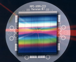
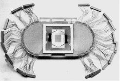
ESA’s XMM-Newton satellite project demanded a challenging large X-ray imager. It became evident that the production of wafer scale defect free novel silicon detectors needed such a well-defined cleanroom environment. In 1990 the technology was transferred to the former premises of the Fraunhofer-Institute for Solid State Technology, based in the Pasing district of Munich. A 250 m2 cleanroom of Class-10 to Class-100 was rented and equipped with fabrication tools for ultra high resistivity float zone silicon. The existing technology was upgraded to four inch wafer size for a fully double sided process. In addition to semiconductor fabrication technology a test area with test benches for the ATLAS strip and pixel detectors was built and an X-ray test facility for the XMM pnCCDs was installed. The simulation and layout tools were upgraded and the implementation of a process data base system for quality assurance and control was realized. In this lab successful realization and implementation of a 36 cm2 pnCCD for XMM was done.
MPG HLL at Neuperlach

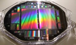
In 1999 we started the evaluation of the upgrade from four inch wafer size (100 mm) to six inch (150 mm). This step was motivated by new projects in need of monolithic detectors larger than six by six square centimeter, the maximum for 100 mm format with a diagonal of approximately 8.5 cm. In 2000 we finished our second facility transfer. This time we moved to the Neuperlach section of Munich on-site the Siemens campus. A 1000m2 of the clean room area, with 600 m2 Class-1 cleanroom was commissioned and qualified in 2001. Again this change of facility was a tremendous step forward in process technology which can be expressed in the following way: In Garching the thermal leakage current per square centimeter – a probe for the quality of the fabrication process – was about 1 nA, in Pasing about 0.5 nA on 280 μm thick detectors. In Neuperlach we routinely achieve 0.1 nA per square centimeter but on 500 μm thick depleted silicon wafers. The smallest structures were going from 3 μm to 2 μm in Pasing. At present they are going to 1.5 μm.
New organization of the laboratory and future plans

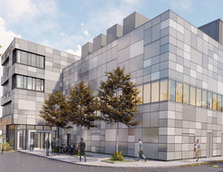
In 2013 organization of the laboratory was changed and MPG HLL became a central facility of the Max Planck Society. Needs for going to even larger area devices continued with time and at present we are in the phase of building our own laboratory with total 1500m2 of the clean room area. We have now returned to the roots of the laboratory's original location in Garching near Munich. On October 7 and 8, we officially inaugurated our new building. We have also upgraded technologically: switching to 8-inch technology and expanding to non-silicon-based devices.