Research and Development Lab
A sandbox for new ideas
Besides the well-controlled, fully qualified, and mostly automated processes in the main cleanroom run by skilled and experienced process engineers, there is also a separated smaller line for experimental processes. This is the R&D and application lab and here new and sometimes wild ideas with non-standard materials and non-qualified processes can be tried out. It is also an educational line where students can do their experiments and get trained to realize their R&D projects. Almost all process modules as in the main cleanroom are available with the main difference that all process steps are done on manual tools. All process tools are set up for 150 mm wafers. However, they could be adapted to processing of 100 mm and 200 mm wafers, and even single die processing can be arranged. Available process modules include:
- Spin coating of a large variety of photo resists with a thickness of about one and up to tens of micrometers, versatile syringe dispense system
- Spin coating of various other functional layers (e.g. BCB, spin-on glass)
- Spray coating of photo resist and functional polymers on wafers with extreme topographies, coating of single dies
- Mask aligner with back side alignment capabilities by IR illumination, also transfer of buried alignment marks within the oxide of a SOI wafers to the wafer surface is possible
- Development of photo resists and other photo-sensitive functional layers by immersion and puddle techniques
- Wet and dry oxidation of silicon up to 1100 °C, annealing of wafers after implantation or sputter processes
- LPCVD deposition of low temperature oxide (LTO), poly-Si, and silicon nitride
- Sputter deposition of Al, Ti:W, Ti, TiN, Cu
- Structuring of functional layers by immersion etch processes
- SF6 and O2 plasma reactor for BCB and photo resist descum process steps
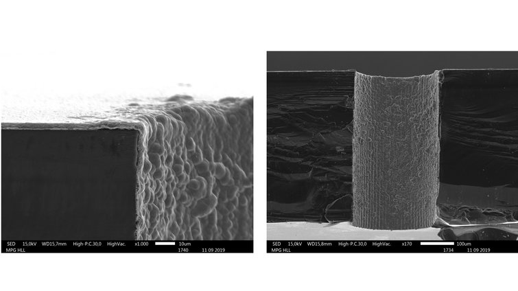
- Deep anisotropic etching of silicon
- Various optical inspection and metrology tools for control and qualification and the functional layers
Among the recent projects in the R&D Lab are
- Feasibility studies on through silicon vias
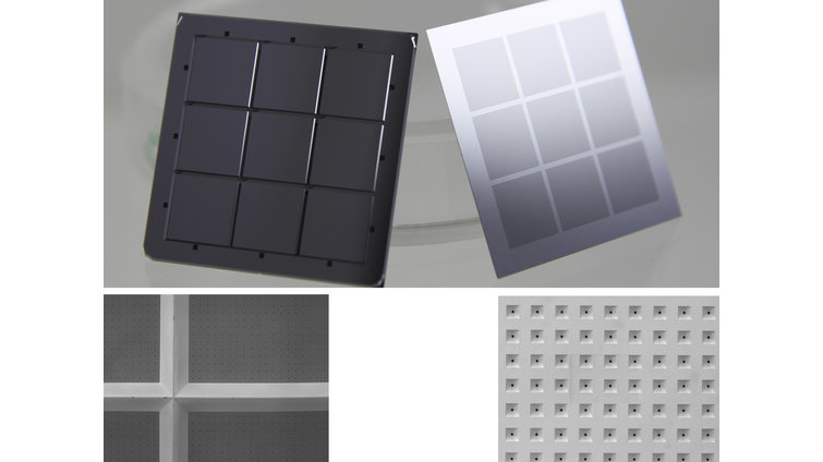
- micro-machined target support structures for various experiments in synchrotron crystallography
- first test application of spin-on glass for planarization
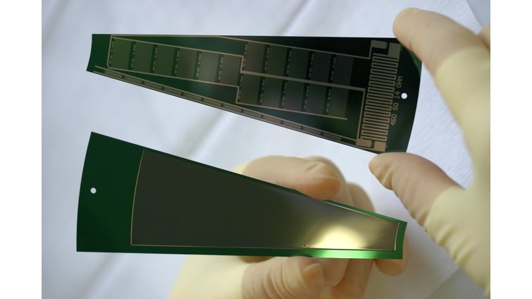
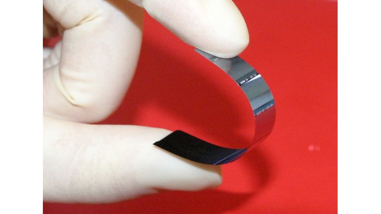
- application of deep anisotropic silicon etching for ultra-thin sensors
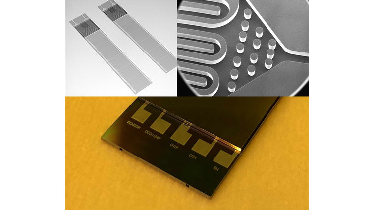
- fabrication of test structures with micro-channel cooling
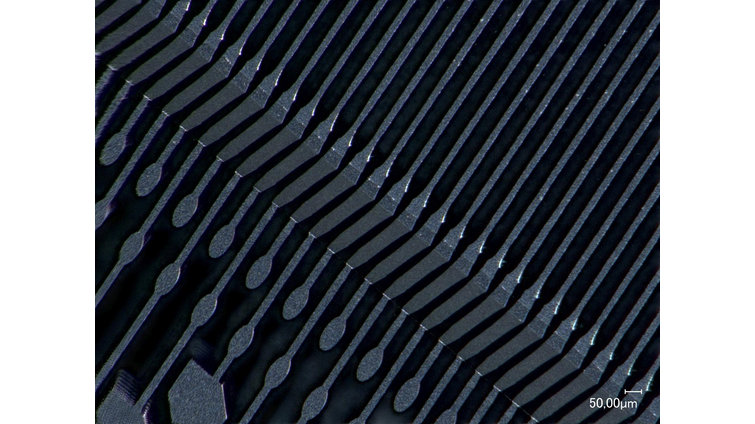
- deposition and structuring of metal lines over extreme topographies.
links:
P. Mehrabi, H.M. Müller-Werkmeister, J.P. Leimkohl, H. Schikora, J. Ninkovic, S. Krivokuca, L. Andriček, S. Epp, D. Sherrell, R.L. Owen, et al.: The HARE chip for efficient time-resolved serial synchrotron crystallography, J Synchrontron Radiat, 27 (2020), pp. 360-370
L. Andricek, G. Lutz, M. Reiche and R. H. Richter, "Processing of ultra-thin silicon sensors for future e+/e- linear collider experiments," in IEEE Transactions on Nuclear Science, vol. 51, no. 3, pp. 1117-1120, June 2004, doi: 10.1109/TNS.2004.829531.
