Charged Coupled Devices
pn-CCDs at the Semiconductor Laboratory
pn-CCDs developed and produced at Max Planck Semiconductor Laboratory are sensors for light and particle detection. pnCCD development at Semiconductor Laboratory started in the late 80s. It was triggered by the ascension of X-ray-astronomy satellites where new semiconductor sensors were needed to lower the detection threshold for soft X-rays.
pn-CCDs are in particular advantageous for X-ray detection. They can be tailored to the needs for X-ray-spectroscopy and X-ray photon counting. In pn-CCDs the storage capacitors are built up with pn-junctions instead of MOS structures. This omits the vulnerable Silicon-Silicondioxid interface making a pn-CCD intrinsically more radiation hard.
In the last three decades we developed and produced many versions of pn-CCDs mainly for the application fields of satellite based X-ray spectroscopy cameras (XMM-Newton, eRosita, EinsteinProbe) and material science (CAMP, LAMP).
Major advantages of pn-CCDs compared to common MOS-CCDs:
- pn-diodes instead of MOS-registers -> better radiation hardness against X-rays and electrons
- deep transfer depth of several microns -> high transfer speed also for larger pixel.
- pn-CCDs can be operated in a high dynamic range mode.
- pn-CCDs have unstructured backside acting as signal entrance window which can be tailored to the needs of the experiment.
- pnCCDs are faster as they use parallel column read out
MOS CCD vs. pn-CCD
The cross sections of the surface regions shown in Figure 1 illustrate the common and different operation principles of both types. Charge is shifted from left to right by applying three periodical voltage clocks (j1,j2,j3) to the metal registers (black - MOS CCD) and p-implants (red - pn-CCD), respectively. Three registers connected to a j triple form one pixel (3-phase CCD). Register clocking shapes the potential within silicon in a way that a staircase like potential distribution is generated in each pixel (Animation pn-ccd2) shifting the electrons to the integrated pre-amplifiers. In contrast to standard MOS CCDs where one pre-amplifier has to read out an entire array or sub array each pn-CCD pixel column has its own readout amplifier which leads to a significantly enhanced readout speed. Figure 1 also shows that the transfer depth is quite differently in both devices.
 and pn-CCD (right)")
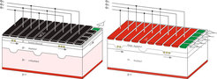
. Electrons are stored in the evolved potential minima beneath the surface. The inset in the foreground shows how electron charge generated in the depth of silicon bulk drifts into the right pixel and is transferred by peristaltically changing potential to the left pixel. (simulated with TeSCA /1/)")

The buried channel type MOS CCD shifts signal charge in a depth of lower than 1µm below Silicon-Silicondioxid interface. The charge transfer depth in pn-CCDs is typically 7µm. A deeper transfer depth is beneficial for a fast readout of larger pixel but is reducing the maximum amount of charge (charge handling capability) which can be stored in a pixel. However, for space-based X-ray telescopes this is an ideal combination. Pixel sizes in the range of about 50µm are usually sufficient in this application field since the X-ray mirrors - limited by size and weight - cannot provide a finer position resolution anyway. For spectroscopy a relative small charge generated by single X-ray photons has to be measured. A charge pile up within pixel by several photons would spoil the information therefore a fast charge transfer and readout is mandatory for the observation of light objects.
 /3/. In the simulation electron charge is transferred back and forth between two neighboring registers of a 51µm pixel. The pixel column in the foreground shows a small charge of about 10000 electrons shifted in the depth 7µm. About 700000 electrons are stored in the registers of the pixel column in the background. First electrons are stored in the deep storage and transfer region. When its storage capability is exceeded storage region extends toward the surface directly beneath the p register doping in a depth of less than 1µm. Note, in both cases charge transfer takes place still in the depth.")

Animation pn-ccd2: Charge transfer in high dynamic range mode based on 3d simulations with Oskar3 by K. Gärtner (WIAS-Berlin) /3/. In the simulation electron charge is transferred back and forth between two neighboring registers of a 51µm pixel. The pixel column in the foreground shows a small charge of about 10000 electrons shifted in the depth 7µm. About 700000 electrons are stored in the registers of the pixel column in the background. First electrons are stored in the deep storage and transfer region. When its storage capability is exceeded storage region extends toward the surface directly beneath the p register doping in a depth of less than 1µm. Note, in both cases charge transfer takes place still in the depth.
Figure 1 shows also the bulk and the backside of the CCDs. pn-CCDs are produced on high-resistivity float-zone n-type silicon with a typical resistivity of about 5kΩcm. The p-doped layer at the backside (Figure 1) and the n-bulk form a diode which fully depletes the whole bulk from electrons at moderate voltage and the entire wafer volume becomes sensitive for incident photons. Charge generated at the backside drifts by the depletion field to the front side, where a confined potential minimum for electrons is created by a low dose high energy phosphorous implant. The peak position of the implant defines the storage and transfer depth of the CCD. The full depletion approach extends the detection range to higher X-ray energies since those X-rays convert deeper in material. But it is also very beneficial for the detection of lower energetic soft X-rays. The sensor backside can be used as radiation entrance window. In contrast to the front side where all electrodes and implant necessary for the CCD operation are located, the backside has to contain only a large p-doped diode layer without obstacles for incident light. By deposition of additional filter layers on top, the entrance window can be tailored to the needs of specific experiments.
Position resolution for X-Ray imaging
For spectroscopic measurements, the pixel size determines how the charge cloud formed in a thick absorbing material is split into detection pixels. If position resolution is of minor importance, large pixels with marginal charge sharing give the best energy resolution and lowest detection threshold. In this case, usually pixel sizes between 50 and 150µm are optimal.
If - in addition to energy and arrival time - also very accurate position resolution is also required, the optimal pixel size depends on photon energy, sensor thickness and electric field strength which together define the size of the charge cloud. The best results can be achieved, if the charge is distributed over 2-3 pixels in each direction. The sum of signals determines the photon's energy while the relative amounts give position accuracy much smaller than the pixel size and mainly limited by proper calibration and readout noise. The optimum pixel size in this application is between 20 and 50µm for a wafer thickness of 0.5mm and a strong electric field with fast charge collection.
The smallest pixel size we realized up to now is 36µm. Based on the knowledge that such charge clouds are inherently Gaussian shaped clever interpolation methods can be applied to achieve position resolutions in the µm range. For a CCD with 36µm pixel size a position resolution of 1.5µm has been obtained by a center of gravity analysis technique /2/.
High charge handling capability mode
The other implication following from the deep charge storage is a rather small capacitance and therefore a small charge handling capability. This usually not an issue for an operation in spectroscopic mode but in the field of material science it limits the number of photons which can be counted and in this way the dynamic range. It seems to be fundamental problem of pn-CCDs but it is not. By applying a larger backside voltage the potential barrier which confines the charge in the deep storage region is lowered and the electrons can be pushed towards the p doped register implant. The charge storage region is vertically extended nearly in the same depth as in a buried channel MOS-CCD. This mechanism is exemplified by the Animation pn-ccd2. Measurements on a pnCCD with 75x75µm² pixel size performed show a large increase of the charge handling capability from 300 hundred thousand to about 2.8 million electrons /4 /.
Further potential of pn-CCDs
Despite of the long successful history the full potential of the pn-CCD detector concept is by far not exploited. The combination of new ideas with new technological options opens the door to better performing detectors and to new applications. Table pn-ccd1 summarizes the characteristics of CCDs which are currently available and the goals we are working on.
Table pn-ccd1: pn-CCD characteristics - state of the art and goals
|
|
Currently available |
Prospective goals |
|
Sensor Size: limited by the wafer diameter |
max. 9x9cm² 150mm |
max. 12x12cm² 200mm |
|
Sensor arrangement Dead space |
max. 4 tiles 2mm |
4-side-buttable ca. 1mm |
|
Storage scheme |
full frame and frame store |
|
|
Pixel size |
36µm … 150µm |
24µm … 150µm |
|
Position resolution Center of gravity method |
1.5µm @36µm pixel size |
<1µm @24µm pixel size |
|
Sensor thickness |
ca. 450µm |
up to 2mm |
|
Noise |
2.5 enc |
< 1enc |
|
Entrance window (dead layer) |
30nm |
ca. 5nm |
|
X-ray energy range @sensor thickness |
90eV - 20keV(50%) @ 450µm |
70eV – 30keV(50%) @2mm |
|
Electron energy range |
5keV…300keV |
|
|
Radiation hardness if on chip electronics is shielded |
radiation hard against soft X-rays and electrons
|
|
|
Charge transfer inefficiency (fraction of lost charge per pixel transfer) |
typ. 3e-5 |
|
|
Charge handling capability |
up to 10^6 electrons (75µm pixel) |
|
|
Operation temperature |
<250K |
≤ RT |
|
Cooling |
Cryostat, Peltier |
Cryostat, Peltier, Multi- Channel-Cooling |
|
Readout scheme |
parallel column readout |
|
|
On chip amplifier |
n-channel JFET |
p-channel Depfet |
|
Readout speed |
5µs /pixel row |
<1µs /pixel row |
|
Readout electronics |
Veritas1, 2 |
Veritas1, 2 … |
In the last three decades we developed and produced many versions of pn-CCDs for a mainly for the application fields of satellite based X-ray spectroscopy cameras (XMM-Newton, eRosita, EinsteinProbe) and material science (CAMP).
External links:
Photoeffect https://en.wikipedia.org/wiki/Photoelectric_effect
CCD https://en.wikipedia.org/wiki/Charge-coupled_device
MOS https://en.wikipedia.org/wiki/MOSFET
Spectroscopy https://en.wikipedia.org/wiki/X-ray_spectroscopy
active pixel sensors https://en.wikipedia.org/wiki/Active-pixel_sensor
Internal links:
radiation entrance window
Simulation https://www.hll.mpg.de/2970734/Simulation
XMM-Newton https://www.hll.mpg.de/2967850/XMM
eRosita https://www.hll.mpg.de/3052840/eROSITA
EinsteinProbe https://www.hll.mpg.de/3052401/Einstein-Probe
LAMP/CAMP https://hll.mpg.de/3053337/LAMP_CAMP
Literature
/1/ H. Gajewski et al, TeSCA – Two Dimensional Semiconductor Analysis Package, Manual, WIAS, Berlin, 1997
/2/ F. Schopper, et al., High resolution X-ray imaging with pnCCDs, Nuclear Inst. and Methods in Physics Research, A (2017), https://doi.org/10.1016/j.nima.2017.10.004.
/3/ K.Gärtner, J. Griepentrog and Th. Koprucki, User documentation Oskar3, Wias-Berlin, 2011
/4/ J. Schmidt et al., Extending the dynamic range of fully depleted pnCCDs
JINST 9 P10008; DOI:10.1088/1748-0221/9/10/P10008