DEPFET Detectors
Being the most consequent application of the principle of sideward depletion, the combined detector-amplifier structure DEPFET is one of the most advanced concepts in the MPG HLL portfolio. DEPFET structures can be used as building blocks for a large variety of different devices ranging from optical photon sensors to X-ray imagers and particle trackers. Due to their extremely low detector capacitance they exhibit excellent signal-to-noise ratio and energy resolution. Currently, DEPFET based active pixel detectors are developed for X-ray astronomy and microscopy, planetology material science and particle physics.
In contrast to CCDs, an active pixel sensor has an integrated amplifier in every pixel, providing in-situ charge amplification. The DEPFET structure combines the features of active pixel sensors, i.e. fast, low-noise, random access readout with the advantages of a sideward depleted device, i.e. full depletion and large sensitive volume.
The term DEPFET (depleted p-channel field effect transistor) refers to a structure consisting of a p-channel field effect transistor, which is integrated on the surface of a high-resistivity, n-type silicon bulk.


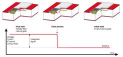
By making use of the principle of sideward depletion, the bulk can be completely depleted, and by applying appropriate potentials, a potential minimum for electrons can be generated, which is located underneath the channel of the FET. The presence of any kind of charge within this potential minimum has an influence on additional charge carriers in the transistor channel, thus modifying its electrical conductivity. Consequently, the presence of charge in the potential minimum has the same effect as the presence of charge on the transistor gate. Therefore, the potential minimum can be considered as an internal gate, while the “classical” gate of a DEPFET is called external gate for distinction. If incoming ionizing radiation generates electron-hole-pairs within the fully depleted silicon bulk, the charge carriers are separated by the electric field, and, while the holes drift towards the p+ contact on the back surface, the electrons are collected in the closest potential minimum i.e. internal gate. The resulting change in the channel conductivity can be used to sense the presence of charge in the corresponding internal gate after converting it to a voltage or current signal. In this way, a DEPFET structure works as a detector for ionizing radiation. The signal can either be obtained directly by continuously observing the DEPFET and detecting the arrival of charge in real time. Alternatively an on-demand measurement can be applied. The difference of the signal before and after removing the charge from the internal gate is now recorded. The charge is removed by a so-called clear structure, which serves as a gateable electron sink. The latter mode is particularly useful when building large area sensors from arrays of DEPFET cells. As the internal gate persists independently from the presence of a transistor current, only one row of transistors within the pixel array can be turned on at a time and their signals are read-out by the described difference method. The process is repeated for all matrix rows. In this way, the interconnection of pixels is feasible, as many transistors can share one common readout contact.
The features of DEPFET based detectors are numerous. Like pnCCDs and other back illuminated detectors, DEPFET based devices are integrated onto a fully depleted silicon bulk. This provides an entrance window with optimum quantum efficiency and a 100 % fill factor.
An extremely low internal gate capacitance yields low noise of the entire detector system. Unlike in a CCD, the charge is stored and amplified in-situ within every pixel and no charge transfer is needed. This is beneficial in terms of radiation hardness, dead time decreases, out-of-time events prevention, fast readout ability as well as pileup probability reduction. As only those pixels are actually turned on, which are currently read out the overall power consumption of the sensor is low. In addition, DEPFET type sensors are very area-efficient, as no frame-store region is needed. Optional windowing and sparse readout can easily be implemented.
DEPFETs can have various topologies and shapes. Being based on sideward depletion, a DEPFET can be used as a readout structure for many types of fully depleted devices, e.g. drift detectors. In this way DEPFET pixel sizes from 20 μm by 20 μm up to about one square centimeter have been realized.
The DEPFET concept is very flexible and serves as a platform for a large variety of new devices and innovative detector concepts, which use the DEPFET as sensitive element.